Author Affiliations
Abstract
1 Wuhan National Laboratory for Optoelectronics, Huazhong University of Science and Technology, Wuhan 430074, China
2 Optics Valley Laboratory, Wuhan 430074, China
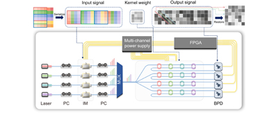
With the advancement of deep learning and neural networks, the computational demands for applications in wearable devices have grown exponentially. However, wearable devices also have strict requirements for long battery life, low power consumption, and compact size. In this work, we propose a scalable optoelectronic computing system based on an integrated optical convolution acceleration core. This system enables high-precision computation at the speed of light, achieving 7-bit accuracy while maintaining extremely low power consumption. It also demonstrates peak throughput of 3.2 TOPS (tera operations per second) in parallel processing. We have successfully demonstrated image convolution and the typical application of an interactive first-person perspective gesture recognition application based on depth information. The system achieves a comparable recognition accuracy to traditional electronic computation in all blind tests.
optoelectronic compute wearable devices micro-ring resonator hand gesture recognition Opto-Electronic Science
2023, 2(12): 230017

Author Affiliations
Abstract
1 School of Electronic Information and Communications, Huazhong University of Science and Technology, Wuhan 430074, China
2 Wuhan National Laboratory for Optoelectronics & School of Optical and Electronic Information, Huazhong University of Science and Technology, Wuhan 430074, China
Metal parts with highly dynamic areas often appear in industrial production measurements. However, if the traditional fringe projection technique is used to project fringe onto the surface of these metal parts, the light energy will be excessively concentrated and the image will be saturated, resulting thus in the loss of fringe information. To effectively address the high reflectivity problem of the object under test in fringe projection, background normalized Fourier transform contouring was combined with adaptive fringe projection in this work and a new method for performing highly dynamic 3D measurements was proposed. To reduce the number of the acquired images by the camera, a monochromatic fringe of different frequencies was put into the RGB channel to make color composite fringe, and then a color camera was used to acquire the deformed color composite fringe map. The images acquired by the color camera were then separated into three channels to obtain three deformed stripe maps. The crosstalk was also removed from these three images, and the 3D shape of the object was reconstructed by carrying out Fourier transform contouring with background normalization. From our experiments, it was demonstrated that the root mean square error of the proposed method can reach 0.191 mm, whereas, unlike the traditional methods, the developed method requires four images.
Highly dynamic objects Adaptive measurement Three-dimensional measurement Three-channel color camera Journal of the European Optical Society-Rapid Publications
2023, 19(2): 2023040
1 Wuhan National Laboratory for Optoelectronics, Huazhong University of Science and Technology, Wuhan 430074, China
2 State Key Laboratory of Advanced Optical Communication Systems and Networks, School of Electronics, Peking University, Beijing 100871, China
In the past half century, silicon-based microelectronics and optical fiber communication have triggered a far-reaching information technology revolution, which has moved human society into a high-speed information age. The demand for communication capacity and speed is growing exponentially. On the other hand, data center and high-performance computing are facing bottlenecks of speed, bandwidth, and energy consumption of electrical interconnections. Siliconbased optoelectronics has become the key technology to break through these bottlenecks. Thanks to the advantages of high refractive index, capable in small active components, and CMOS compatible process, silicon can achieve a largescale optoelectronic integration on a micro-chip with low cost and low energy consumption. This has become a hot alternative for the chip industry. In addition, silicon-based optoelectronics has enabled a series of new study fields such as mid-infrared communication, microwave optoelectronics, lab-on-chip, quantum communication, optoelectronic computing, and chip scale lidar.
Frontiers of Optoelectronics
2022, 15(2): s12200
华中科技大学 武汉光电国家研究中心, 武汉 430074
硅基集成光子器件具有体积小、集成度高的突出优势, 在光通信、数据中心光互连等领域具有广阔应用前景。然而, 硅基波导耦合器件尺寸相对较大、工作带宽和工艺容差受限。硅基多模路由光子器件设计还面临挑战。文章介绍了近年来发展起来的两种硅基集成光子器件先进设计方法: 绝热捷径法和变换光学方法, 简要阐述其物理原理, 并展示在硅基集成光子器件设计中的典型应用。
硅基集成光子器件 绝热捷径法 变换光学方法 silicon-based integrated optical devices shortcuts to adiabaticity transformation optics

Author Affiliations
Abstract
1 Wuhan National Laboratory for Optoelectronics & School of Optical and Electronic Information, Huazhong University of Science and Technology, Wuhan 430074, China
2 Hubei Key Laboratory of Intelligent Wireless Communications, College of Electronics and Information Engineering, South-Central University for Nationalities, Wuhan 430074, China
Multimode waveguide bend is one of the key components for realizing high-density mode-division multiplexing systems on chip. However, the reported multimode waveguide bends are either large, bandwidth-limited or fabrication-complicated, which hinders their applications in future high-density multimode photonic circuits. Here we propose a compact multimode waveguide bend supporting four TE modes simply by shape-optimizing with transformation optics. The shape of the waveguide is optimized in the virtual space with gradient distribution of the refractive index, so that the scattering loss and intermode cross talk are well suppressed. After conformal mapping back into the physical space, a compact (effective radius of 17 μm) multimode bending waveguide is obtained. Simulations show that the proposed multimode waveguide bend has little loss () and low cross talk () throughout an ultrabroad wavelength range of 1.16–1.66 μm. We also fabricated the shape-optimized multimode bending waveguide on a silicon-on-insulator wafer. At 1550 nm wavelength, the measured excess losses for the four lowest-order TE modes are less than 0.6 dB, and the intermode cross talks are all below . Our study paves the way for realizing high-density and large-scale multimode integrated optical circuits for optical interconnect.
Photonics Research
2020, 8(12): 12001843
Wuhan National Laboratory for Optoelectronics, School of Optical and Electronic Information, Huazhong University of Science and Technology, Wuhan 430074, China
Frontiers of Optoelectronics
2019, 12(2): 148–156

Author Affiliations
Abstract
1 Wuhan National Laboratory for Optoelectronics, School of Optical and Electronic Information, Huazhong University of Science and Technology, Wuhan 430074, China
2 State Key Laboratory of Optical Communication Technologies and Networks, Wuhan Research Institute of Posts and Telecommunications, Wuhan 430074, China
3 e-mail: xxiao@wri.com.cn
Photonic-assisted microwave frequency identification with distinct features, including wide frequency coverage and fast tunability, has been conceived as a key technique for applications such as cognitive radio and dynamic spectrum access. The implementations based on compact integrated photonic chips have exhibited distinct advantages in footprint miniaturization, light weight, and low power consumption, in stark contrast with discrete optical-fiber-based realization. However, reported chip-based instantaneous frequency measurements can only operate at a single-tone input, which stringently limits their practical applications that require wideband identification capability in modern RF and microwave applications. In this article, we demonstrate, for the first time, a wideband, adaptive microwave frequency identification solution based on a silicon photonic integrated chip, enabling the identification of different types of microwave signals from 1 to 30 GHz, including single-frequency, multiple-frequency, chirped-frequency, and frequency-hopping microwave signals, and even their combinations. The key component is a high Q-factor scanning filter based on a silicon microring resonator, which is used to implement frequency-to-time mapping. This demonstration opens the door to a monolithic silicon platform that makes possible a wideband, adaptive, and high-speed signal identification subsystem with a high resolution and a low size, weight, and power (SWaP) for mobile and avionic applications.
Photonics Research
2019, 7(2): 02000172
Author Affiliations
Abstract
1 College of Information Science and Technology, Nanjing University of Aeronautics and Astronautics, Nanjing 210016, China
2 College of Electronics and Information Engineering, Nanchang Hangkong University, Nanchang 330063, China
3 Key Laboratory of Nondestructive Test (Ministry of Education), Nanchang Hangkong University, Nanchang 330063, China
4 Wuhan National Laboratory for Optoelectronics, Huazhong University of Science and Technology, Wuhan 430074, China
We discuss the optimal design of line-tapered multimode interference (MMI) devices using a genetic algorithm (GA). A 1×4 MMI device is designed as a numerical example. Compared with the conventional design based on self-imaging theory, the present method demonstrates superior performance with low insertion loss and small non-uniformity.
平面波导器件 多模干涉耦合器 遗传算法 230.1360 Beam splitters 230.7390 Waveguides, planar 310.2790 Guided waves Chinese Optics Letters
2009, 7(11): 1045
Author Affiliations
Abstract
1 Wuhan National Laboratory for Optoelectronics, Huazhong University of Science and Technology, Wuhan 430074, China
2 State Key Laboratory on Advanced Optical Communication Systems and Networks, Peking University, Beijing 100871, China
3 School of Electrical and Computer Engineering, Georgia Institute of Technology, Atlanta, Georgia 30332, USA
A high-permittivity (high-k) material is applied as the gate dielectric layer in a silicon metal-oxide-semiconductor (MOS) capacitor to form a special electro-optic (EO) modulator. Both induced charge density and modulation efficiency in the proposed modulator are improved due to the special structure design and the application of the high-k material. The device has an ultra-compact dimension of 691 \mu m in length.
硅基调制器 电光调制器 高K栅层 MOS电容 230.4110 Modulators 250.4110 Modulators 250.6715 Switching 230.2090 Electro-optical devices Chinese Optics Letters
2009, 7(10): 924
Author Affiliations
Abstract
1 Wuhan National Laboratory for Optoelectronics, College of Optoelectronic Science and Engineering, Huazhong University of Science and Technology, Wuhan 430074, China
2 Faculty of Mechanical and Electronic Information, China University of Geosciences, Wuhan 430074, China
3 State Key Laboratory on Advanced Optical Communication Systems and Networks, Peking University, Beijing 100871, China
4 School of Electrical and Computer Engineering, Georgia Institute of Technology, Atlanta, Georgia 30332, USA
A novel microring resonator accelerometer is proposed. It is realized by a suspended straight waveguide coupled with a microring resonator. Under the external acceleration, the coupling coefficient is a function of gap spacing between the two waveguides. The mathematical model of the sensing element is established. Both the finite element method and coupled mode theory are adopted to analyze and optimize the proposed structure. Simulation results show that the mechanical sensitivity is 0.015 \mu m/g with the working frequency below 500 Hz and cross-axis sensitivity less than 0.001%, which is promising in seismic related applications.
加速度 微环谐振器 有限元法 耦合模理论 130.6010 Sensors 230.5750 Resonators Chinese Optics Letters
2009, 7(9): 798


